[TIL] How to generate custom footprints in KiCad
![Cover Image for [TIL] How to generate custom footprints in KiCad](/_next/image?url=%2Fassets%2Fblog%2Fkicad-custom-footprint%2Fcover.png&w=3840&q=75)
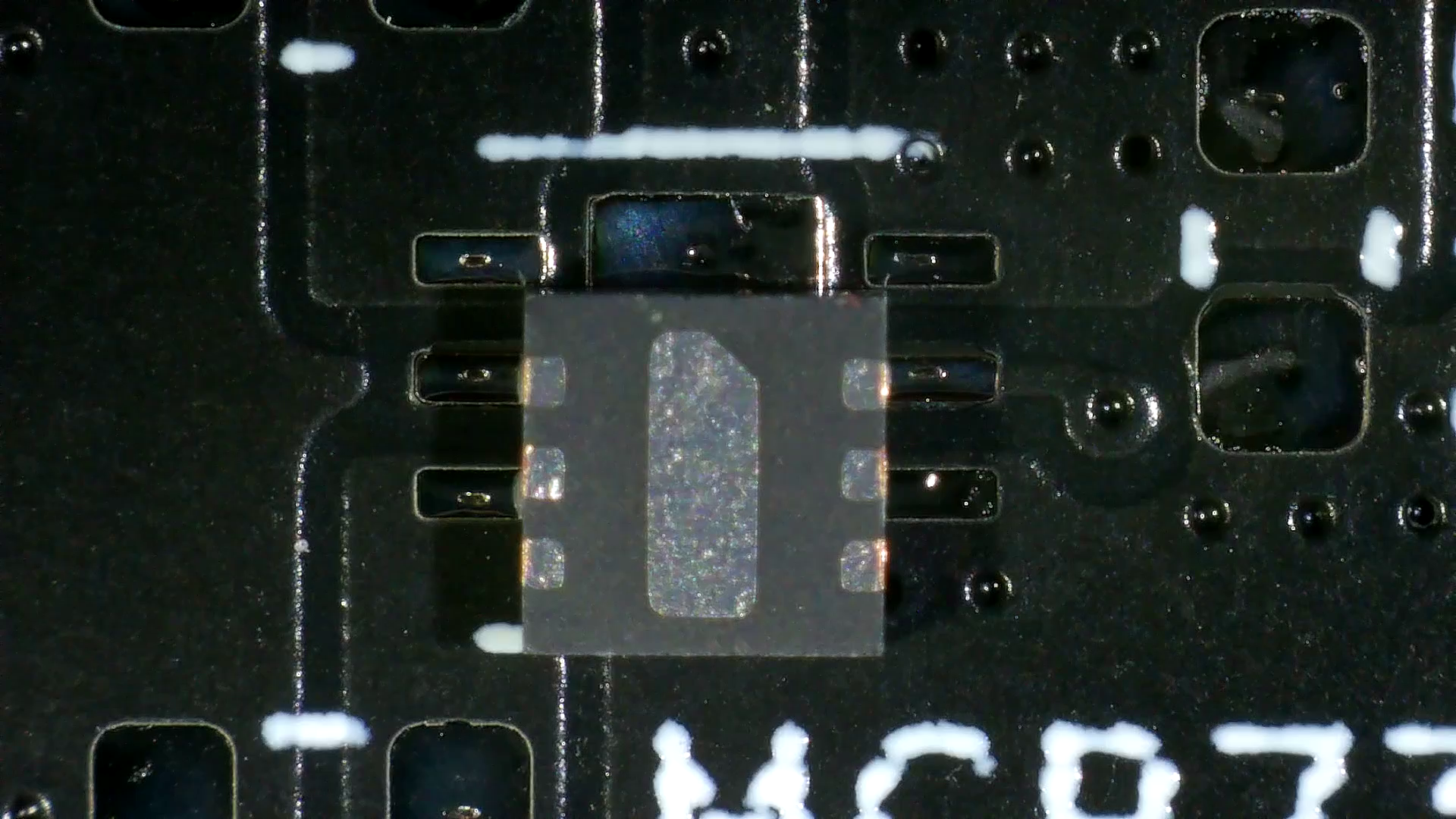
I was debugging a new PCB that I developed a couple weeks back. The LiPo charger IC would just not charge the battery. I was probing the board with an oscilloscope, trying to debug with a thermal camera and looking at the data sheet over and over again. And then it hit me, did I perhaps select the wrong footprint? I did and I needed to update the board. That should be an easy fix except that KiCat didn't have the footprint I needed.

I needed a TDFN-6-1EP_2x2mm_P0.5mm_EP0.6x1.6mm and all I got was a TDFN-6-1EP_2.5x2.5mm_P0.65mm_EP1.3x2mm. And that's the one I was using initially. I didn't think hard enough at the time and clearly missed that the IC would not fit at all. Now I had to go and copy the existing one and go through the hassle of making the necessary adjustments. But while doing so I noticed this line in the footprint’s description:
TDFN, 6 Pin (http://www.nve.com/Downloads/ab3.pdf), generated with kicad-footprint-generator ipc_noLead_generator.pyGenerated. To my surprise, there is a repository of scripts that generates all kinds of footprints and it should be very possible to generate the one I needed too. What follows are the steps I took to get my footprint.
- Check out KiCad Footprint Generator.
- Navigate to the script for the footprint category you're after. For me that was
scripts/Packages/Package_NoLead__DFN_QFN_LGA_SON/size_definitions/dfn.yaml. - Add the footprint of your choice to the YAML file copying from a similar footprint.
- Run the script responsible for the footprint category you're using. For me that was
python ipc_noLead_generator.py size_definitions/dfn.yaml. - Import the footprint in question into KiCad.
- Success ✨